Menu

Ultra-high Res FESEM | SEM5000X

Ultra-high Res FESEM | SEM5000X

Ultra-high Resolution Field Emission Scanning Electron Microscopy (FESEM)

Product information

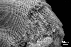
The CIQTEK SEM5000X is an ultra-high resolution FESEM with optimized electron optics column design, reducing overall aberrations by 30%, achieving ultra-high resolution of 0.6 nm@15 kV and 1.0 nm@1 kV.

Its high resolution and stability make it advantageous in advanced nano-structural materials research, as well as the development and manufacturing of high-technology node semiconductor IC chips.


Electron Optics

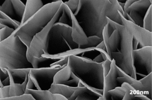
Objective Lens Upgrade

Lens chromatic aberration was reduced by 12%, lens spherical aberration was reduced by 20%, and overall aberration was reduced by 30%.


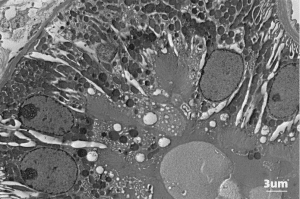
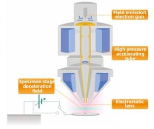
Dual Beam Deceleration Technology

In-lens beam deceleration, applicable to specimens with large volumes, cross-sections, and irregular surfaces. Dual deceleration technology (In-lens beam deceleration + specimen stage tandem beam deceleration) challenges the limits of specimen surface signal-capturing scenarios.


Software options

  • Particle & Pore Analysis Software (Particle) *Optional
    The CIQTEK SEM Microscope software employs various target detection and segmentation algorithms, suitable for different types of particle and pore samples. It enables quantitative analysis of particle and pore statistics and can be applied in fields such as materials science, geology, and environmental science.
  • Image Post-processing Software *Optional
    Perform online or offline image post-processing on images captured by electron microscopes and integrate commonly used EM image processing functions, convenient measurement, and annotation tools.
  • Auto Measure *Optional
    Automatic recognition of line width edges, resulting in more accurate measurements and higher consistency. Support multiple edge detection modes, such as Line, Space, Pitch, etc. Compatible with multiple image formats and equipped with various commonly used image post-processing functions. The software is easy to use, efficient, and accurate.
  • Software Development Kit (SDK) *Optional
    Provides a set of interfaces for controlling the SEM microscope, including image acquisition, operating condition settings, power on/off, stage control, etc. Concise interface definitions allow for the rapid development of specific electron microscope operation scripts and software, enabling automated tracking of regions of interest, industrial automation data acquisition, image drift correction, and other functions. Can be used for software development in specialized areas such as diatom analysis, steel impurity inspection, cleanliness analysis, raw material control, etc.
  • AutoMap *Optional

Features

* optional


Image Gallery

Mesoporous Silica 1 kV (Duo-Dec) / lnlens
Kidney Sections 5 kV / BSED-COMP
Nickel Foam 2 kV / ETD-SE


Downloads

No downloads found.